A smartphone display may look simple from the outside.
Behind the glass, however, there is a highly complex stack of optical films, adhesives, shielding layers, diffusion materials, protective liners, and touch-sensitive components. These layers must work together with extremely high accuracy to deliver the bright, clear, and reliable screen experience consumers expect.
In consumer electronics, even a small dimensional error can create a visible defect.
A fraction of a millimeter may determine whether a screen looks premium or defective. This is why precision film die cutting has become an essential manufacturing process for modern electronic displays.
From smartphones and tablets to smartwatches, laptops, OLED displays, and foldable devices, manufacturers rely on precision die-cut film components to improve display quality, assembly efficiency, and long-term product reliability.
At Sanken, we often work with customers who find that display performance depends not only on the material selected, but also on how accurately that material is converted into finished components.

What Is Precision Film Die Cutting?
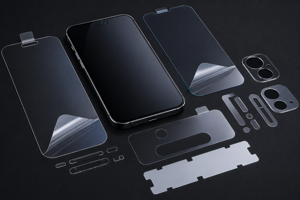
Precision film die cutting is the process of converting thin functional materials into accurate shapes, openings, layers, and finished components.
These materials may include:
- Optical films
- PET protective films
- Diffuser films
- Reflective films
- Brightness enhancement films
- EMI shielding films
- Insulation films
- Double-sided adhesive tapes
- Release liners
- Surface protection films
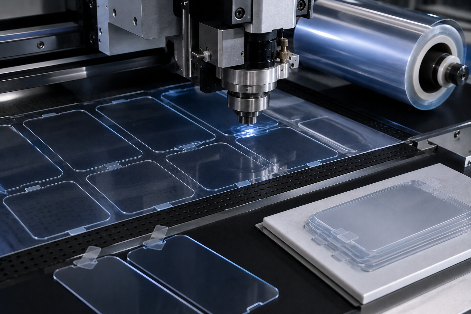
Using precision tooling and controlled converting processes, manufacturers can create film components that match the exact geometry required inside electronic devices.
Unlike simple cutting, precision die cutting focuses on tight tolerance control, clean edges, repeatable dimensions, and stable mass production.
For modern consumer electronics screens, this accuracy is not optional. It directly affects display appearance, assembly yield, and product reliability.
Why Display Components Require Extreme Accuracy
Consumer electronics are becoming thinner, lighter, and more compact.
At the same time, screen modules are becoming more complex. A typical display structure may contain several functional layers, each with a different purpose.
| Display Layer | Main Function |
|---|---|
| Cover glass | Surface protection |
| Optical adhesive | Bonding and optical clarity |
| Touch sensor | User input |
| Polarizer film | Light control |
| Brightness enhancement film | Display brightness |
| Diffuser film | Light uniformity |
| Reflective film | Light efficiency |
| Protective film | Surface protection during assembly |
Each layer must align correctly with the display area, camera opening, sensor window, speaker cutout, and housing structure.
If one layer is slightly misaligned, the result may include:
- Light leakage
- Visible gaps
- Uneven brightness
- Bubble formation
- Touch sensitivity issues
- Assembly failure
- Cosmetic defects
Precision film die cutting helps ensure each film layer fits exactly as required before it enters final assembly.
Improving Display Appearance
Consumers judge electronic devices visually.
A screen is one of the first areas customers notice. Even small defects can create the impression of poor quality.
Poorly converted film components may cause:
- Rough film edges
- Misaligned openings
- Visible dust or particles
- Uneven borders
- Optical distortion
- Poor edge appearance
These problems become more obvious in high-resolution screens, OLED displays, tablets, smartwatches, and premium smartphones.
Precision die-cut film components help manufacturers achieve clean, consistent, and professional screen appearance. This is especially important for brands that compete on visual quality and user experience.
Supporting Ultra-Thin Device Designs
Modern consumer electronics continue to become thinner.
Manufacturers want slimmer smartphones, lighter tablets, compact smartwatches, and thinner laptops. However, every internal layer still needs to perform its function.
Precision film die cutting helps product designers reduce unnecessary material and optimize the use of limited internal space.
It allows manufacturers to:
- Remove excess film area
- Create accurate openings
- Reduce assembly interference
- Support compact component layouts
- Maintain function in thin structures
For ultra-thin devices, poor film conversion can create stacking problems, edge lifting, or interference during assembly. Accurate die cutting helps each layer fit smoothly into the final product structure.
Enhancing Assembly Efficiency
Consumer electronics manufacturing often involves high-volume production.
Millions of display modules may be assembled within a short production window. If film components are inconsistent, production speed and yield can be affected.
Poorly converted films may lead to:
- Difficult positioning
- Manual adjustment during assembly
- Higher labor cost
- Increased rejection rate
- Slower production speed
- Unstable automated assembly
Precision die-cut components improve positioning consistency and make it easier for operators or automated equipment to place each part correctly.
This supports:
- Pick-and-place accuracy
- Faster assembly
- Better repeatability
- Lower scrap rates
- More stable mass production
For OEMs and electronics manufacturers, assembly efficiency is not only about speed. It also affects cost, delivery time, and customer satisfaction.
Protecting Sensitive Display Components
Display modules contain delicate surfaces that can be easily damaged during handling, transportation, and assembly.
Sensitive areas may include:
- Polarizer films
- Optical coatings
- Touch sensor layers
- Brightness enhancement films
- Protective glass surfaces
Precision die-cut protective films are often used to prevent scratches, dust contamination, fingerprints, and surface damage.
These protective films must be shaped accurately. If the film is too large, it may interfere with assembly. If it is too small, it may fail to protect the required area.
Precision die cutting ensures protective films match the exact surface area they are designed to cover.
Supporting Advanced Display Technologies
Display technology continues to evolve quickly.
Modern products may use:
- OLED displays
- Mini-LED displays
- Micro-LED displays
- Flexible screens
- Foldable displays
- Curved display modules
- Touch-integrated screen structures
These technologies often require more complex film shapes and multi-layer constructions.
Precision die cutting supports advanced display designs by enabling:
- Complex geometries
- Narrow borders
- Accurate sensor openings
- Multi-layer film registration
- Flexible material conversion
- Consistent adhesive placement
Foldable and flexible displays create even higher requirements because materials must bend, move, or remain stable under repeated use. In these applications, poor cutting accuracy may lead to edge stress, delamination, or long-term reliability problems.
Why Clean Edges Matter
Edge quality is a critical factor in film die cutting.
A film component may look simple, but poor edge quality can create serious production and reliability issues.
Common edge-related problems include:
- Burrs
- Loose particles
- Rough edges
- Adhesive residue
- Film tearing
- Delamination risk
For optical and display applications, contamination from poor cutting edges can become visible inside the screen.
Precision die cutting helps create smooth, clean, and stable edges. This reduces particle generation and supports better long-term reliability.
Clean edges are especially important when processing optical films, adhesive films, and thin protective films used inside consumer electronics screens.
Contamination Control Is Equally Important
Dimensional accuracy alone is not enough for display applications.
Cleanliness is just as important.
Dust particles trapped inside a display assembly may cause bright spots, dark spots, visible marks, or customer complaints.
High-quality film converting may require:
- Clean room production
- Anti-static control
- Protective liners
- Controlled material handling
- Proper packaging
- Dust prevention during processing
For optical films and display components, contamination control should be considered from material storage to die cutting, inspection, packaging, and delivery.
At Sanken, we understand that display components must meet both dimensional and cleanliness requirements. A part that is accurate but contaminated may still fail in final assembly.
Why Adhesive Integration Requires Precision
Many display film components include pressure-sensitive adhesive layers.
These adhesive layers must align with display structures, sensor windows, camera openings, speaker openings, and bonding areas.
Poor adhesive alignment can cause:
- Weak bonding
- Adhesive overflow
- Visible residue
- Assembly interference
- Functional failure
- Cosmetic defects
Precision die cutting helps control both the film shape and the adhesive shape.
For multi-layer adhesive film structures, registration accuracy is especially important. Each layer must stay aligned during lamination, cutting, waste removal, and final packaging.
This is one reason why material converting experience matters. The challenge is not only cutting the film, but also controlling the complete process.
Reducing Material Waste
Optical films, protective films, and functional display materials can be expensive.
Precision die cutting helps reduce waste by improving material utilization and reducing scrap.
This can support cost control through:
- Better nesting layout
- More stable cutting performance
- Lower defect rates
- Less material loss
- Improved production yield
For high-volume consumer electronics programs, even a small improvement in yield can create meaningful cost savings.
However, cost reduction should not come at the expense of quality. The right converting partner should balance material efficiency, dimensional accuracy, cleanliness, and production stability.
What Buyers Should Check Before Ordering Die-Cut Display Films
Before placing an order for precision die-cut film components, buyers and engineers should confirm several important details.
| Item to Check | Why It Matters |
|---|---|
| Film material type | Different films require different cutting methods |
| Thickness tolerance | Affects stacking and assembly |
| Adhesive structure | Influences bonding and release performance |
| Dimensional tolerance | Determines fit and alignment |
| Edge quality | Reduces particles and defects |
| Cleanliness requirement | Important for optical display applications |
| Delivery format | Rolls, sheets, kits, or custom packaging |
| Inspection standard | Helps control mass production quality |
Clear specifications help reduce trial time, avoid misunderstanding, and improve production results.
For display projects, it is also useful to provide drawings, samples, material datasheets, assembly requirements, and expected production volume.
How Sanken Supports Consumer Electronics Display Projects
Sanken provides precision die cutting and material converting solutions for consumer electronics display applications.
Our capabilities include:
- Precision film die cutting
- Optical film converting
- Protective film processing
- Multi-layer lamination
- Adhesive integration
- Clean room manufacturing
- Kiss cutting and through cutting
- Custom packaging and delivery formats
We support components used in:
- Smartphones
- Tablets
- Smartwatches
- Laptops
- OLED display modules
- Foldable devices
- Touch screen assemblies
- Consumer electronics modules
Our team helps customers convert advanced film materials into stable, accurate, and assembly-ready components.
By combining material knowledge, tooling control, clean handling, and production experience, Sanken helps manufacturers improve display quality and reduce manufacturing risk.
Conclusion
Precision film die cutting plays a critical role in modern consumer electronics screens.
It affects display appearance, assembly efficiency, contamination control, adhesive performance, material waste, and long-term reliability.
As devices become thinner, smarter, and more visually demanding, the accuracy of each film layer becomes increasingly important.
For smartphones, tablets, smartwatches, OLED displays, and foldable devices, precision die-cut film components help ensure that advanced screen designs can be manufactured reliably at scale.
At Sanken, we support consumer electronics manufacturers with precision film die cutting, clean room production, adhesive integration, and custom converting solutions for high-performance display applications.